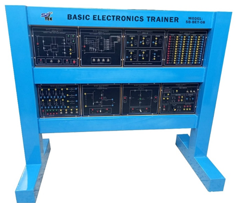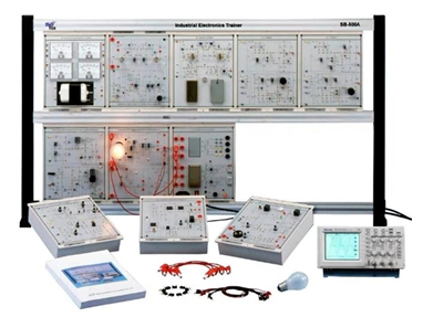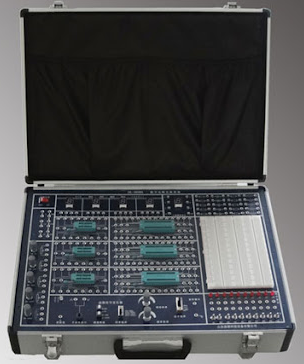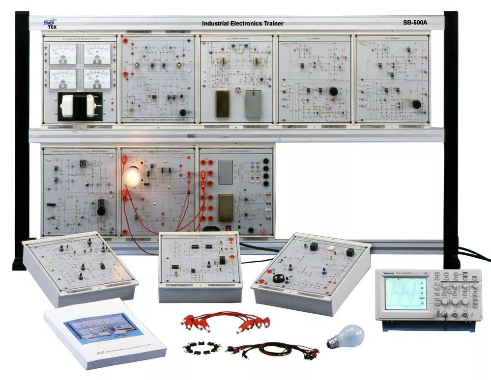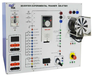
Specification:
Power Supply Bank: Constant Voltage Output: ±5V, ±12V. Variable Voltage Output: 0V ~ 48V. Power source: 220~230V AC, 50Hz, 1 Phase. Constant Voltage Output: 9V-0-9V. Constant Voltage Output: 24V, 3-Phase. Power source: 380~440V AC, 50Hz, 3 Phase
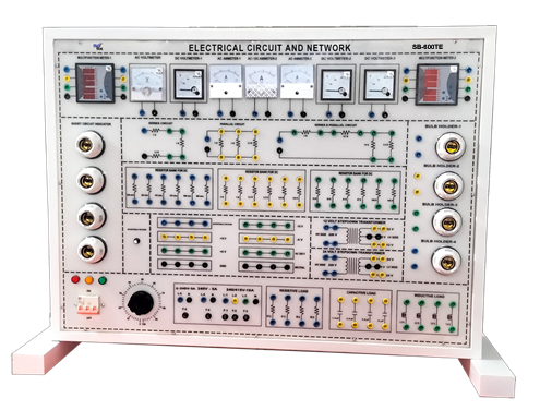
Multimeter Bank:
DC Voltmeter, Range (0-50V). DC Ammeter, Range (0-100mA). AC Voltmeter, Range (0-50V). A Digital Multimeter
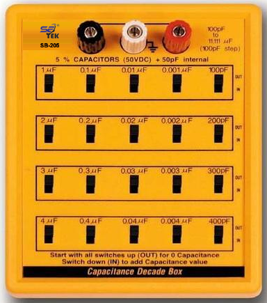
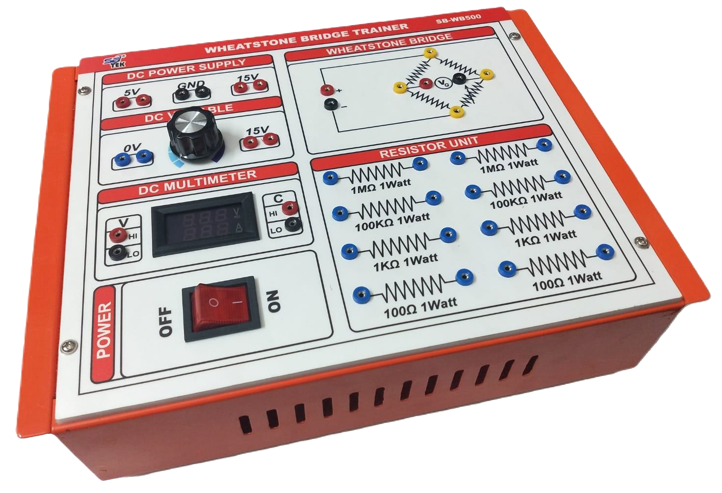
RLC and Potentiometer Bank:
Resistor: 22k-2p,1k-2p,10k-2p,2.2k-2p,4.7k-2p,3.3k-2p.
Inductor: 90uh-1p,470uh-1p,1uh-1p,10uh-1p.
Capacitor: 10uf-2p, o.o1uf-2p, 22uf-2p, 0.1uf-2p, 4.7uf-2p, 1000uf-2p.
Potentiometer: 1k-1p, 10k-1p, 100k-1p, 500k-1p, 1M-1p.
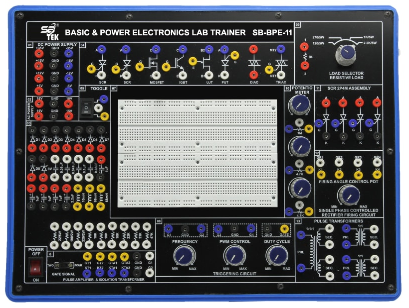
Power Diode
Rated voltage: 600V, Rated current: 10A. Power Diode biasing experiment.
Power Diode characteristic experiment. Power Diode rectification experiment.
SCR Bank
4-amp 600V general-purpose Silicon Controlled Rectifiers is up to 400Hz on resistive or inductive load. High surge capability. High on-state current. High stability and reliability. SCR Principle. SCR characteristic curve. SCR Construction. SCR trigger mode. SCR RC phase control circuit. SCR biasing experiment. SCR characteristic experiment. SCR controlled rectifier experiment.
DIAC Bank:
VBO: 32 V and 40 V. Low breakover current. Breakover voltage symmetry: 3V.
Diac biasing experiment. Diac characteristic experiment. Application of Diac.
TRIAC Bank:
Gate Turn-On Voltage (Vgt): 1.5V. Peak Off-State Voltage (Vdrm): 500V. On-State Current (It): 4.0A. Gate Current (Igt): 25mA. Typical Voltage Change over Time (dV/dT): 250V/µs. TRIAC biasing experiment. TRIAC characteristic experiment. TRIAC AC wave controlled. Application of TRIAC. Control Lamp, TRIAC Control Speed Experiments. TRIAC shift control. TRIAC automatic control lamp experiment. TRIAC control motor speed experiment.
MOSFET Bank
The MOSFET has a maximum Vds of 55V. Maximum drain current (Id) of 48A. Maximum power dissipation (Pd) of 625W. It is capable of fast switching speeds and low on-resistance, for high-power switching applications. MOSFET biasing experiment. MOSFET characteristic experiment. MOSFET speed control experiment.
IGBT Bank:
600V 6.5A Power IGBT operating frequencies 8-40kHz in hard switching, >200kHz in resonant mode. IGBT biasing experiment. IGBT characteristic experiment. IGBT speed control experiment.
Power Transistor Bank:
Collector-Base Voltage:100V. Collector-Emitter Voltage:100V. Emitter-Base Voltage (IC = 0): 5V. Collector Current 5A. Collector Peak Current 8A. Base Current 0.1A. Power Transistor characteristic experiment. Power Transistor control experiment.
LIST OF Extra EXPERIMENTS:
Single-Phase Rectifiers (AC-DC)
(1) Single-Phase Half-Wave uncontrolled rectifier
(2) Single-Phase Full-Wave uncontrolled rectifier
(3) Single-Phase Half-Wave controlled rectifier
(4) Single-Phase Full-Wave controlled rectifier.
Three-Phase Rectifiers (AC-DC):
(1) Three-Phase Half-Wave uncontrolled rectifier.
(2) Three-Phase Full-Wave uncontrolled rectifier.
(3) Three-Phase Half-Wave controlled rectifier.
(4) Three-Phase Full-Wave Semi-Controlled rectifier.
(5) Three-Phase Full-Wave Fully-Controlled rectifier.
Three Phase Rectifier & Filter:
(1) Power input: 10 or 30, 0-220V AC
(2) With Inductor & capacitor filter circuit
(3) Surge voltage protection circuit
(4) Output voltage: 0-300Vdc (max.)/10A(max.)
Three Phase Angle Controller
(1) Pulse output: Electric isolation, can directly drives up to 6 thyristors
(2) Trigger angle: 0~180
(3) Control input signal: 0-10V
(4) Rectification angle: 0~90 adjustment
(5) Convert angle: 0~180 adjustment
(6) Working voltage: ±15V, single pulse & continuous pulse.
Buck-Boost Switching Power Supply Unit
(1) Test point: Switching control IC output signal. Current feedback signal. Voltage feedback signal. Switching power component terminal.
(2) Switching frequency: 240KHz.
(3) Converter control: Isolation feedback converter.
(4) Input voltage: DC 20~30V.
(5) Output: 60W, up to 85% efficiency.
(6) Output voltage ripple: ?5%.
(7) Output voltage regulation: ?5%.
(8) Output voltage: DC 25V-30V, adjustment.
(9) Rated current: 2A Max. Overload & short circuit protection
(10) Switching power component: MOSFET.
DC PWM Generator
(1) Triangular wave (carrier) generator: Amplitude: ±10Vp or 0~10Vp. Frequency: 1k, 10k, 15kHz
(2) PWM Signal generator: 2PWM control signal
(3) Working power supply: DC plus/minus 15 * V / 0.5 * A.
Single Phase PWM Controller)
(1) Triangular wave(carrier) generator: Amplitude: ±10Vp. Frequency: 1k, 5k, 15kHz.
(2) Sine wave signal generator
(3) Multiplex
(4) PWM Signal generator: 2 x TTL level
(5) Square wave signal generator
(6) Working power supply: DC ± 15V
Step Up and Step Down Chopper Unit
(1) Test point: Switching control IC output signal. Current feedback signal. Voltage feedback signal. Switching power component terminal.
(2) Switching frequency: 240KHz.
(3) Converter control: Isolation feedback.